
Project:
ecgc
Date:
15/01/2024
Finished assembly of hardware re-re-redesign
Hurray, it works!
It goddamn works!
I have finally received the PCBs and components and have soldered them.
And it justs works!!!
Yeah baby!!!

Anyhow, enough celebrating. Let me elaborate on the current progress and process.
Assembly process
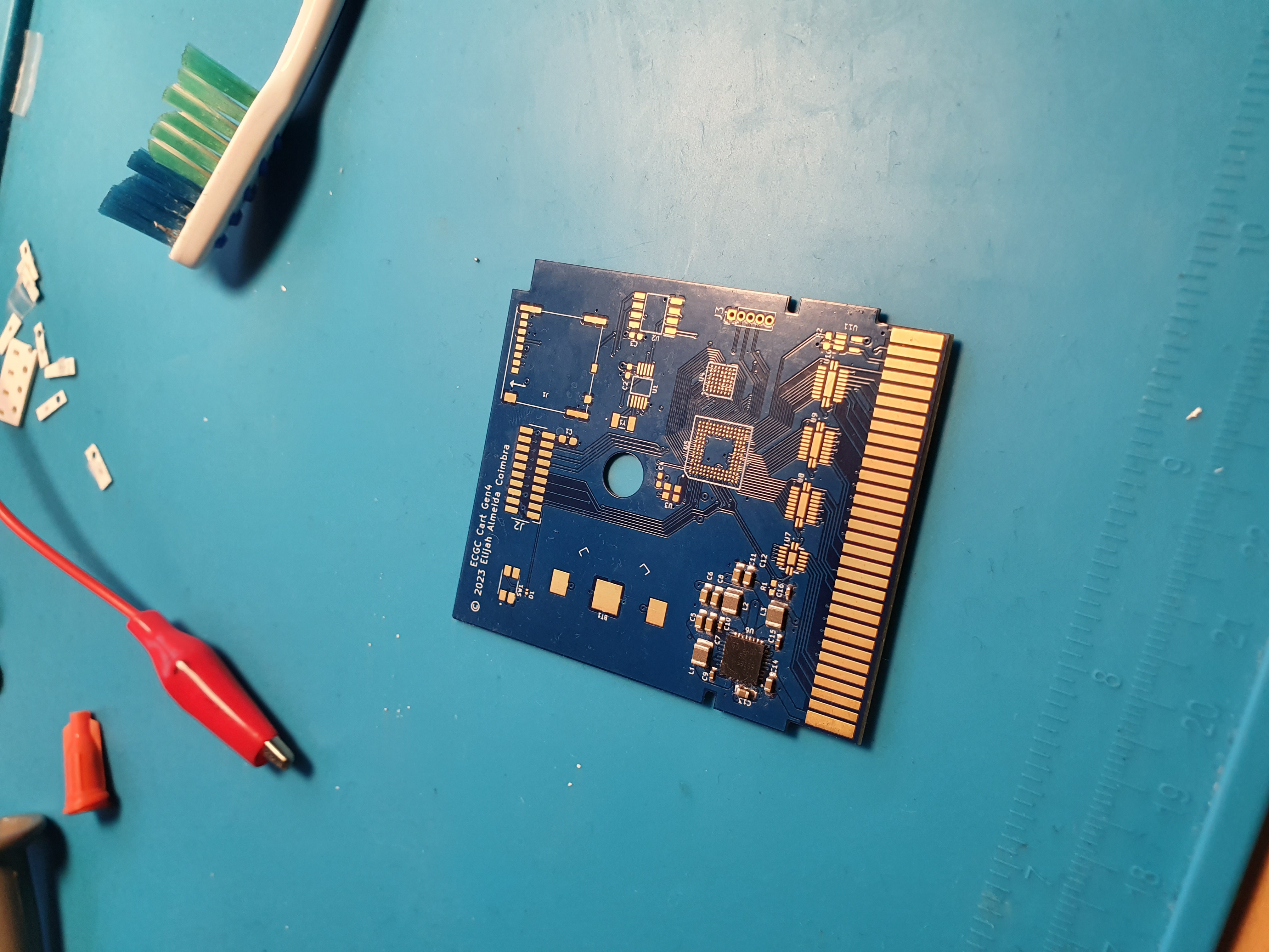
As said prior, I have soldered all components on the PCB. I have pictures below of the assemblies.
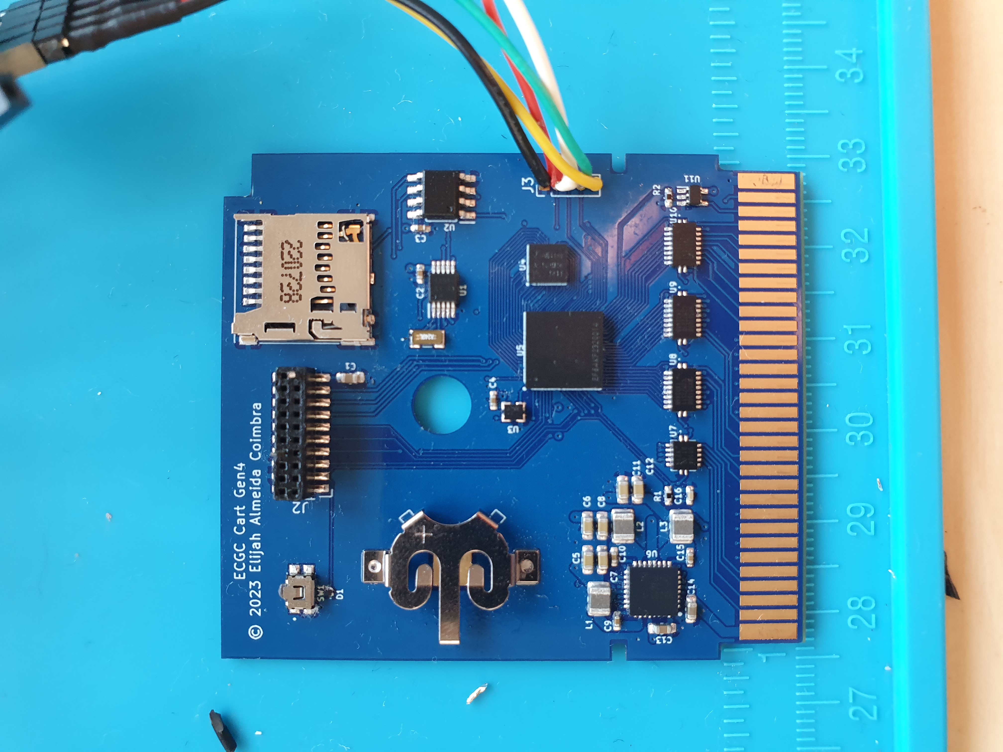
Soldering them was easier than expected. I kept delaying it due to being afraid of soldering the FPGA wrong and burning it. However, it seems I was a coward and I succeeded in the first try (yeah me).
The entire assembly process took about 6 hours. I started first with sorting inventory and getting everything I needed. I have a soldering mat with numbered pits which I used to keep the components sorted.
After finishing inventory, I applied the soldering paste using a stencil on the top layer. It did take me 2 tries, since I had the stencil misaligned a bit when applying the paste on my first try. I cleaned the PCB with a bit of IPA and contact cleaner to remove all paste before trying for a second time.
I then placed all components on the freshly applied paste. This took an extremely steady hand and keeping my breath. Minor misalignments were corrected with gently bumps using my tweezers. I have to say, I am so glad I bought a new microscope. My old one was a cheap ~€15,- USB microscope from Aliexpress. I now bought a more decent ~€150,- USB/HDMI microscope, with which I can actually see what I'm doing on.
Then, I placed the board on the bed of my 3D printer to pre-heat the board to 80°C. When the bed achieved the desired temperature, I blasted the board with my hot air station on 400°C till all the solder was melted. In the process though, I melted the reset button (SW1) and the expansion board connector (J2). The expansion port was fine though, only having its plastic smoothed. The button was ruined however. Luckily, I ordered spares, plus I can just short the button pads using tweezers in a pinch (pun not intended).
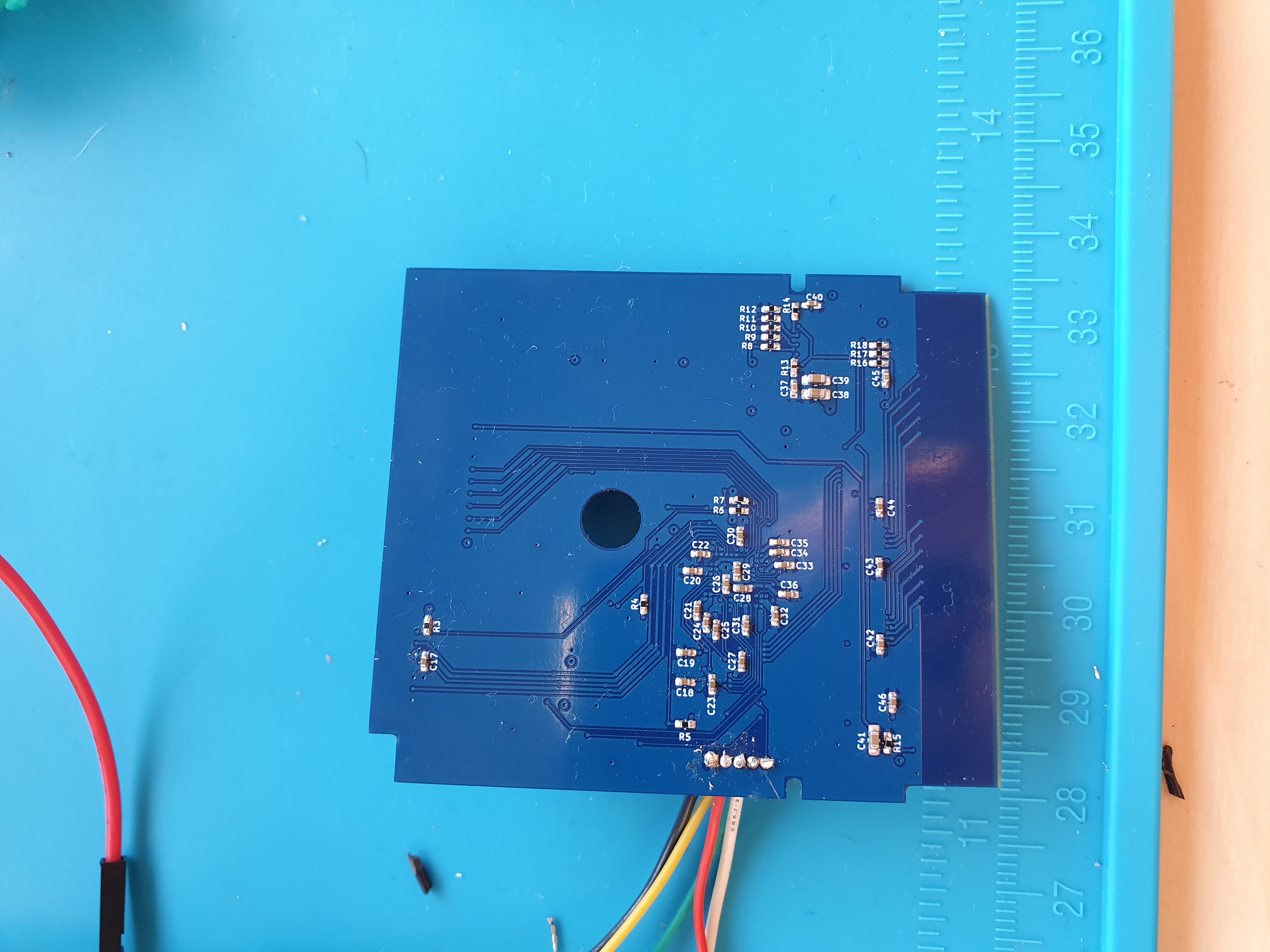
I did the same for the bottom side. However, without the pre-heating since the board did not lay flat anymore. I also did not want to risk the FPGA getting burned. This did not go was well as the top side. I blew a capacitor and resistor off the board (C34 and R7), which I re-soldered by hand. You can see my messy hand work on the pictures if you look closely.
Finally, after extensive visual inspection, the assembly was done!
Experimenting with the power supply
Prior to soldering the entire assembly, I made a version where I only soldered minimum necessary components to get the power supply running. I was not sure if I did my calculation correctly and actually get the appropriate voltages. In the case that I did fail in my calculations, I did not want to potentially destroy ~€50,- worth of components. This also served as a soldering experiment, to try out the soldering method I wanted to use.
As a soldering method, I used the same as described in Assembly Process, with some minor deviations. In the power supply only run, I applied solder paste manually using a syringe. Depending on the size of the components (I only had 0402 and 0603 packages on the backside), I placed a small dot on both pads. The syringe point was not small enough to apply it on the individual pads. Then using my tweezers, I cut the dot in half and push the material on top of the pads.
I thought that applying solder paste on the backside with the stencil was impossible. After soldering the topside, the board does not lay flat anymore, which I thought made using the stencil impossible. However, it just made it more difficult. Laying the PCB on the J2 connector to make it level and some careful holding of the stencil, I was able to place the stencil flat on the backside for the complete assembly process.
After soldering the components, I tested the power supply with my lab power supply, connecting the cartridge pads to +5V. However, there was a short on one of the enable pins to ground, which made the cartridge sink current to ground, resulting in a current draw of ~500mA and the power supply IC making a weird high-pitched humming noise. After much finicking with my smallest soldering tip, I was able to break this bridge, and the supply worked as intended.
I also did some current drawing tests. Nothing too complicated, just connecting my lowest valued resistor to the power supply output and ground, and seeing if the voltages dropped or fluctuated in unexpected ways. I did not have much at hand, only a couple of 5Ω 5W resistors. I was able to pull only ~400mA at most from the +3V3 supply rail. Nothing exploded and I was satisfied with just this.
Testing the assembly
After having made the assembly, I of course proceeded testing it. For this, I devised a simple testing procedure. Each procedure increased in coverage and complexity. If the previous test fails, one should stop and solve the issues of said test before continuing.
Test 1: Visual inspection
Before anything, a quick visual inspection should take place. It is a quick way to test for any solder bridges, improper connections or missing components.
Using a microscope (or a magnifying glass, may god help you), check all components and solder connections. When encountering any defects, fix them using an appropriate method. When all looks well, proceed with the next test.
Test 2: Testing against shorts
Another basic test, is a test for shorts on the power rails. There are few connections to test and the results could be catastrophic if it fails, therefore it is a good idea to do this. Using a continuity meter, I tested all power nets for the following:
- A power net may not have a low resistance path to GND.
- A power net may not have a low resistance path to a different power net.
The power nets in question were the following:
- +5V coming from the Gameboy cartridge pins.
- +3V3 at the filtered power supply output from LX1 of U1 (place a probe on L1).
- +1V8 at the filtered power supply output from LX3 of U1 (place a probe on L2).
- +1V2 at the filtered power supply output from LX2 of U1 (place a probe on L3).
If none of the power nets fail the conditions, the test is a success.
Test 3: Testing the power supply
After checking against shorts, one should connect the Gameboy VCC and GND to a +5V power supply to test the power supply.
One thing to look for is the idle power draw. The idle power draw should give an indication of the state of the components. If for example, a component has been burned by the soldering process, the power draw would be abnormally high. Using a different example, if the current draw is too low, a component might not have been soldered correctly despite looking like it is.
IMPORTANT!!!: if the current draw is abnormally high (>500mA), immediately disconnect power. Something is shorted and the high current draw might destroy components on the board.
Currently, I am not sure what the expected current draw is. The current assembly draws ~30-45 mA when idle. I haven't been able to test all components however, so I am not sure whether this is expected. However, since nothing blew up, I trust that this value should not be too far off.
If power draw looks plausible, check if the power rails all have the correct voltages (see the power rails mentioned in Test 2). If one of more of the power supplies have the incorrect voltage, it can mean a number of things. Most probable, a power supply component may be soldered wrong (e.g. incorrect resistor for feedback, resulting in the wrong programmed voltage). Investigate further what the issue might be.
Test 4: Test the JTAG connection
With JTAG, one can connect to the FPGA and perform many functions (e.g. reading status information and uploading an image). Attempting to use this port can determine if the FPGA works properly and has not been damaged.
To perform this test, simply try to retrieve status info from the FPGA.
Using the Diamond Programmer in the Lattice Diamond software suite,
Perform an action such as SRAM Read DONE bit or SRAM Read Status Register
and confirm that the operation is successful.
If the software fails to retrieve this info, the FPGA might be bad or not soldered properly. Further investigation is needed to determine the exact cause.
Test 5: Functional test of FPGA image
If JTAG is working, one can finally proceed to program the FPGA and check the Gameboy functions. The current firmware and bootloader image is pretty bare bones, but if it runs successfully, it confirms the proper operation of many components and shows that the data path between the Gameboy and FPGA functions.
TODO: show working cart with GB
If something is wrong with the cartridge data path, the bootloader will fail to run. This might be expressed in a number of ways:
- Gameboy is stuck with a blank or corrupted screen.
- Gameboy is stuck on its starting screen.
- The
Nintendo©logo might be corrupted, blacked or blanked out.
- The
In these scenarios, there might be an issue with multiple things:
- The Gameboy reset might not work properly. Check the reset buffer and its connections.
- The FPGA clock might not output a clock signal. Check the clock generator and its connections.
- The FPGA reset might be stuck. Check the reset button and its connections.
- The image might have been corrupted. Check the DONE and INIT bit status and consider re-uploading the FPGA image.
- The bus transceivers might not work properly. Check them and their connections.
In any case, investigate further what the root cause might be.
Future plans
Now that I have functioning hardware close to the end product, I can focus again on the firmware. I have already modified the firmware for Gen3Prototype to run on the current generation. However, this is only a bare bone version. I have removed the audio controllers, debug core and DRAM controller, leaving the rest as is or with minor modifications. I also refactored the firmware to a new coding standard to hopefully improve readability.
The current plans for the firmware moving forwards are:
- Modifying the debug core to work over serial instead of SPI. I now realise that SPI was a poor fit due to it needing an intermediary (it being an Arduino). Using serial, I can connect a serial-to-USB board directly to the FPGA, cutting the complexity of the debug bus.
- Designing and implementing a new RAM controller. Since I have a new RAM chip with an interface differing from the previously used DRAM, I have to make a new controller core for Wishbone mastering. I have already started on this. The new RAM has 2 operating modes: asynchronous and synchronous. The initial mode is asynchronous and I have already implemented this, however I'd like to use synchronous mode to make use of bulk reads/writes. This, coupled with a caching system might make the system more responsive and efficient. But that's a decision for future me.
- Implement other necessary cores.
These include:
- A GPIO core for the SPI slave selects.
- A SPI master core for mastering the different SPI devices.
- An RTC core compatible with MBC3.
After all this, I plan to work on testing using software. I want to implement a BIST (Built-In Self Test) in the bootloader for quick verification. But this is after the firmware is mostly complete.
Closing remarks
Aaah, I am soo satisfied with the current state of affairs. I was stressing a whole lot about the hardware, wondering if I stupidly connected a trace wrong somewhere. Seeing the finished assembly just brings me so much joy and excitement for the future. I spark has ignited within me baby, and this is just the beginning!