
Project:
ecgc
Date:
06/11/2023
Almost done with hardware re-re-redesign
Hello again dear reader. I have worked on the hardware design for the last month or so and almost have it. At the time of writing, I have completely revised the previous schematic and developed a new generation to be made into a PCB. I've included pictures below of the (almost) final product.
Everything is essentially there, I just need to perform some final checks. I don't want to have ordered the PCB and then find out I forgot to route a signal. I normally wait about a week before ordering. If I don't find anything within that week, the PCB is ready to go! I am however sad at the price. Didn't expect for the PCB to cost ~€330,- and that is considered cheap. Apparently, I need to pay a bit of a premium because of my tight tolerances.
But enough about that, let's talk about the redesign in detail.
Deviations from original plan
First, I want to discuss some deviations from the original plan. While looking at the schematic, I saw some stuff I wanted to change. Since making Gen3, I have learned more about electronics and with that experience, I saw a couple of things I wanted to change. I won't mention minor things like pin re-assignments, just the larger changes.
Changed bus transceivers
The biggest change is the switch to a different bus transceiver. Originally, I used the SN74LVCH16245A. It consisted of 2 8-bit transceivers with 5V tolerant inputs. I used this chip because I saw it used on some other Gameboy flash cartridge. However, the issue with this part is that it only down-translates from 5V to 3V3. 3V3 signals stay at 3V3. This works with the original Gameboy TTL hardware, but would not work with a modern Gameboy made with an FPGA using CMOS technology.
Furthermore, the chips were HUGE compared with other components. The new FPGA would be a fraction of the size of just 1 transceiver. Thus, I searched for a replacement. I settled on the NXS0108BQX and NXS0104BQX. The only difference between the two is that the 108 has 8 IO pins, while the 104 has 4. They can provide voltage translation both ways and are much smaller.
Added external clocking
I decided to include room for an external clock. I found it weird that one would use external clocks when chips generally have internal oscillators. After looking online for a bit and talking to a colleague at work, I found out that this is because external clocks are more precise. I thought that maybe the DRAM issues could have come from an unstable clock. Seems unlikely, but it doesn't hurt to include one in the design.
The only issue I have with it is that the clock I chose pulls 23mA at 1V8, which increases our power consumption. It's not horribly much, but is still some power draw. I'll determine during some experiments if the clock is really necessary, otherwise it can just be left out from the board.
Added expansion port breakout
For this prototype, I decided to include an expansion port. This is mainly for getting access to some important signals during development (e.g. DONE, INIT, RESET, etc.). But, one could also maybe use it as an expansion port for extra hardware. Some games include extra hardware. For example Kirby Tilt 'n' Tumble, which included accelerometers for motion controls.
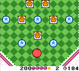
The game loop consisted of the player controlling Kirby as a rolling ball through puzzles. The player could move Kirby by tilting the Gameboy. Additionally, the player could flick the Gameboy to make Kirby jump. To enable such games on the system, I thought it interesting to have some FPGA pins exposed so that myself (or others) could develop their own modules).
The expansion port includes the following:
- Power pins (3V3 and ground)
- User pins (these can be programmed in the FPGA fabric to do anything)
- Soft reset (for resetting the FPGA)
- Programmer DONE pin (detecting if the FPGA is programmed)
- Programmer INIT pin (putting the FPGA in programming mode + detecting if the power supply is good)
- FPGA Test Output Enable (which tri-states all FPGA pins)
- SPI bus (for controlling external peripherals + access to SPI programming)
- Gameboy audio pin
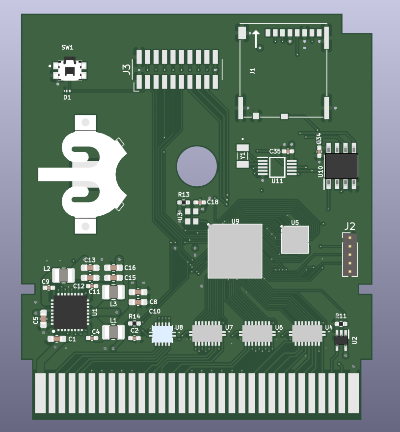
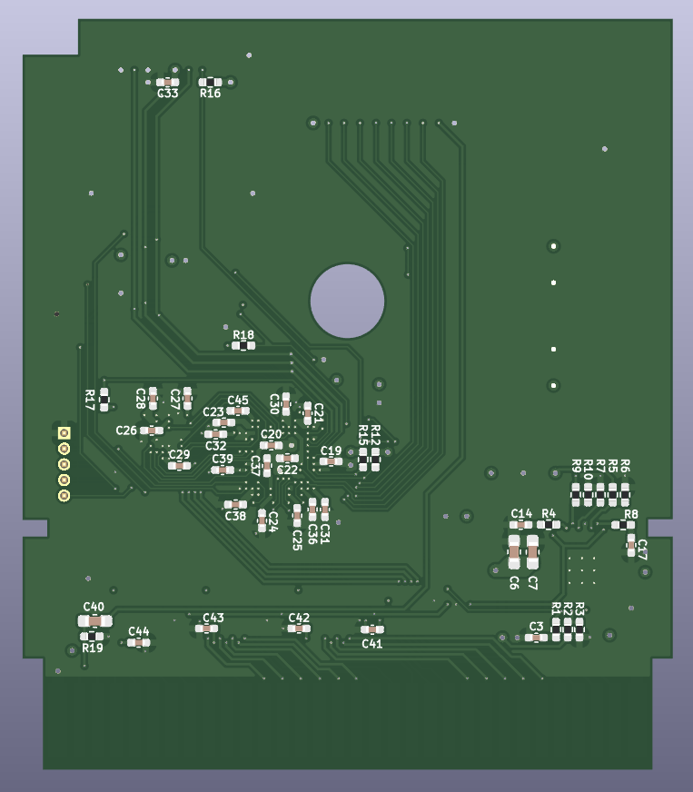
PCB overview
I've marked the PCB top with the important regions. All components mentioned in the last post are here with the same reasoning. The bottom of the cartridge mainly has decoupling capacitors and pull-up/down resistors.
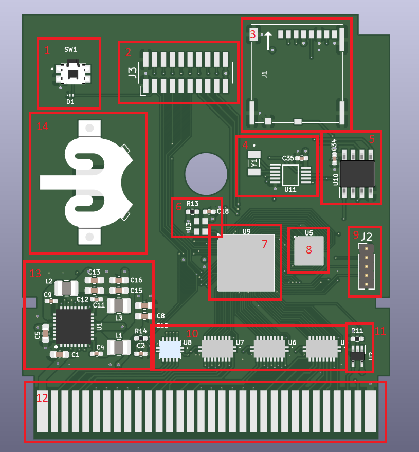
- Reset switch
- Expansion header
- SD card holder
- Real-time clock
- NOR flash
- External 33.333333 MHz oscillator
- FPGA
- PSRAM
- JTAG header
- Bustransceivers
- Reset buffer
- Cartridge connector
- Power supply
- RTC battery
Closing remarks
I am very happy with the current progress. I thought I'd have less time and motivation, but it was really enjoyable lately to work on the project and was able to finish it faster than expected. I will probably write the next post after having soldered everything, ported the old firmware to work on the new hardware and can boot from the boot rom. I'll see what I'll do from there after having done that. Probably getting the RAM to work.
Anyhow, see you in a few weeks/months!