
Project:
ecgc
Date:
18/09/2023
Hardware re-re-redesign
Hi all, back again from vacation. I have spent some time working on other stuff and I felt motivated again to work on the project, so here we are!
Some might have noticed the site being down for a some time (~1 month). I was working on remodelling my room and completely forgot to turn on my server again. I currently have it setup temporarily under my mom's desk, since my room is not yet finished. But it will be staying there for a while till I finish my room, where I'll move it to my room and the server will live there for the foreseeable future.
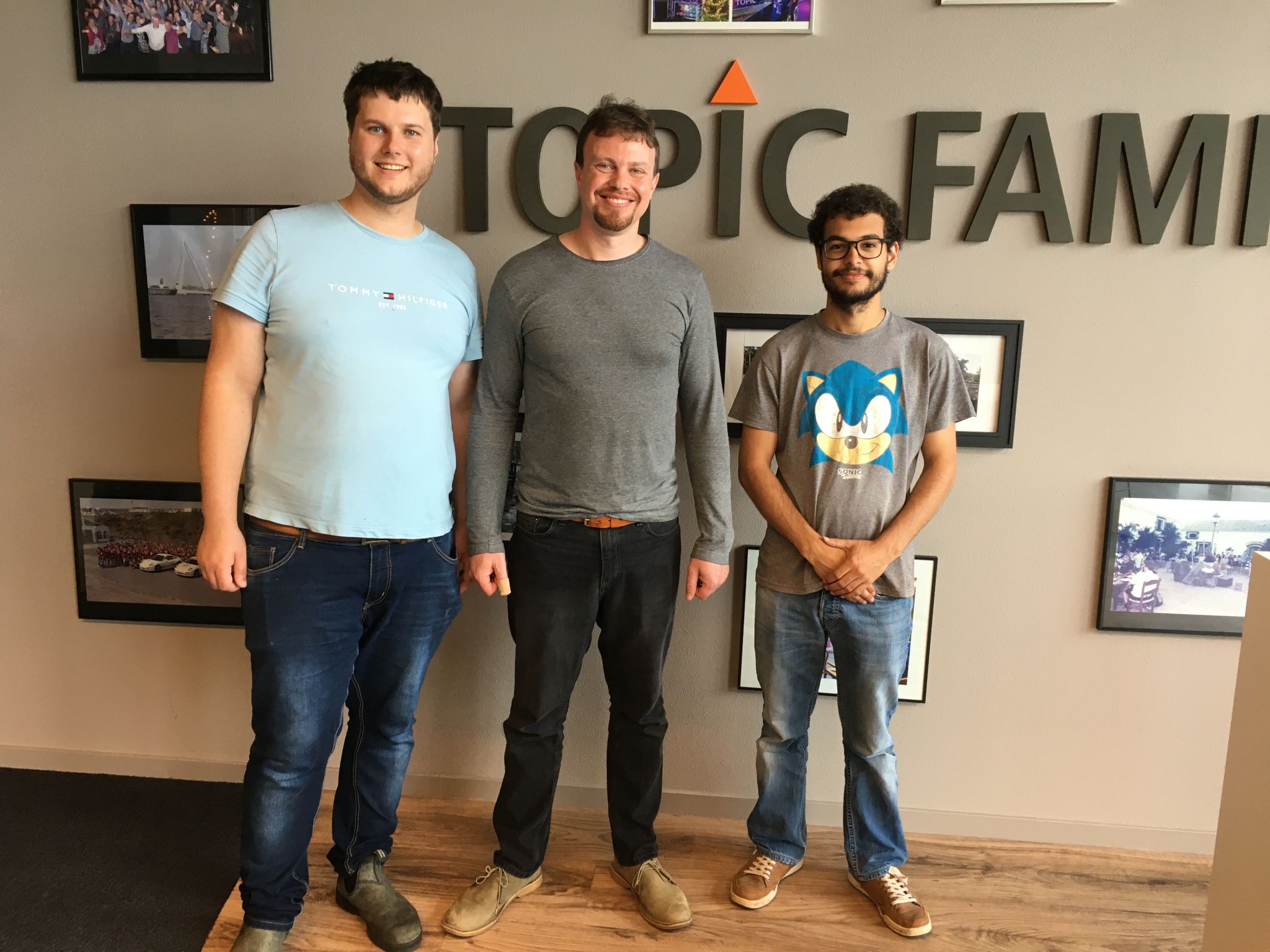
I am currently working on my graduation internship at Topic Embedded Systems, where I'll spend the next 6 months as a Junior Firmware Engineer. I added a picture below with myself and some new colleagues.
I was working on FPGA stuff and felt the need to start on this project again. I have been doing some reflecting and I think that it is time for a new hardware iteration. More importantly, I think I want to change the FPGA.
Thoughts on the current generation
Before talking about the current generation, I want to first set the scene as to why it is what it is.
The current generation, Gen3, uses the MachXO3D family of FPGA's as the main muscle of the operation. At the time, I had started thinking about using micro-controllers to create a custom cartridge. But later down the line, I had heard about FPGAs, which I thought were pretty neat and could implement the features I wanted better. I could implement bus decoding logic, memory mapping, co-processing and more, all without breaking a sweat. At the time, I had also started an internship at EVS Broadcasting Equipment, where I had an assignment with heavy involvement of FPGA's. This made me consider the usage of FPGA's and led me to create Gen3.
At the time, I was an absolute beginner in FPGA's. So when selecting one, I just picked one that seemed to have enough features for what I wanted and was available. I just wanted an FPGA which I could prototype on and was a likely candidate to use on the final product. This was also around the Corona lockdown, so the chip shortage was running rampant.
Looking back, I don't think I would have picked a different FPGA, but I am starting to feel the annoyance of the current prototype. When working on the audio controller, I faced the issue of not having DSP cores. Modulating volume and mixing signals would have been much easier using simple multiplications with DSP cores. I also plan to have an ALU with multiplication in the future, which would be better to implement using a DSP.
I am also having issues with the PCB. For one, the constant instability issues, mainly with DRAM. These issues will most likely be fixed when designing a proper PCB and having everything soldered properly.
I also think I'll give up trying to get the DRAM to work. Using the current methods, there are already many memory errors and no hope to implement double speed mode.
So long story short, I think the current generation has served its purpose by giving me the necessary hindsight. It was still a very useful generation, since it did give me a platform to develop most of the basic features on. A huge improvements over the other 2 generations...
Plans for the next generation
My next efforts on the project will be to redesign the hardware (again) and create a PCB assembly close to the final product. It will be small enough to fit into a cartridge shell. This won't enable me to change wirings on the fly anymore, but I don't think I have to at this point. I just want a stable PCB which I can develop on.

So I developed a design for the hardware above. Many things will be the same. The FPGA will be a different model, but still implement the same functions. The 2 bus transceivers used for level translation also remain the same. The reset architecture also. I think I will also add the audio hardware designed during my last efforts, although I will first see if it even fits and tweak it assuming I have DSP cores.
RAM
Now for the differences. First of all the most important component: the RAM. As mentioned previously, I want to ditch DRAM. From testing, it was deemed unreliable (although it is most probably due to my bad PCB design). And most important, the solution was barely fast enough during normal operation, but no way I will be able to implement double speed mode. So I am currently looking at PSRAM, since it is cheaper than straightup SRAM, but boasts similar speeds and simplicity.
I am considering the AS1C8M16PL-70BIN. It has the necessary 8MB for implementing the MBC5, with and additional 8MB for other stuff. Mainly, a 128KB chuck can be used for save data in the MBC5. It also boasts a 70ns access time, which should be enough for my application. The only caveat is that the chip works on 1.8V logic levels, which will complicate my power supply design.
FPGA
The FPGA I am considering is the LFXP2-8E-5MN132C from the LatticeXP2 Family. It is a bit smaller than the MachXO3D I am currently using, both in physical size (8x8 instead of 10x10) as in LUT count (8k instead of 9.4k). It also has half of the BRAM, having 221kb instead of 432kb. It is missing some features, like the user flash and hard-end SPI controller. But to compensate, it has 4 DSP blocks. It also has DDR2 support baked in, but I won't use it. The FPGA is also slightly cheaper (about €5 at the time of writing).
The missing features will need to be compensated for. The missing UFM will be handled by an external EEPROM instead. Luckily, the LatticeXP2 does have boot flash, so I don't need that. The SPI controller will need to be implemented in firmware.
Power supply
The power supply is new, since I didn't need to design one with the breakout board. The FPGA works with 1.2V levels internally, but the IO to the Gameboy will need to be done using 3.3V. This is the maximum voltage levels the FPGA IO pins can handle and is high enough for the TTL logic to correctly detect. Also for the new PSRAM chip, I need 1.8V power and IO.
This means I need a supply that can convert 5V from the Gameboy Vcc to 1.2V, 1.8V and 3.3V. For this, I have chosen the TPS65266-1RHBT. It is a switch mode power supply with 3 independent outputs. It can accept 2.7V to 6.5V and output 0.6V to 5.5V at 3A/2A/2A. The amperage is a bit overkill, but the chip boasts 90+% efficiency and is pretty cheap.
RTC and battery
Some MBC's provide an RTC for time management, so I've added one to the cartridge as well. I have never experimented with it before, but I had bought the DS1391U-33+, since it seemed like a good fit.
It can be communicated with using SPI, which means I can reuse the SPI core for the SD card. It also provides hardware for battery switching and management.
For the battery, I will choose the largest one that fits. I'd like for the RTC to be able to work for at least 1 year before having to recharge it.
SD card
Of course, we have the SD card for loading games. The cartridge will have a slot for inserting said card. The card will be communicated with using SPI, since it is a simple protocol and has decent enough speeds for our application.
EEPROM
The EEPROM will be used to save non-volatile data used by the cartridge bootrom. The idea is to save the bootloader on the EEPROM and load it at boot into RAM. I might also use the EEPROM for other stuff, like save character sets and splash screens, but I prefer having some simple memory onboard for future use. Something like 64kB might be more than enough. If it does proof to be difficult however due to PCB size limits, I do not mind dropping this.
Closing remarks
So yeah, I'll be busy for the upcoming months on the hardware redesign. Although, I won't have that much time since I still need to finish my room and now also have my internship to worry about. I plan to make a post when I have the new hardware design finished, or maybe somewhere in between if I have enough to say.