
Project:
ecgc
Date:
21/02/2024
Firmware development report
Back again with a new update. I made some progress on the firmware I mentioned in my last post and I wanted to document this. I have made some good progress, including installing and testing the controller for the new PSRAM. Let me take you along on what I have done so far.
New UART-based debug controller
The first point I mentioned in my last post was the debug controller. I had an architecture where I could communicate with a debug core using SPI. My PC does not have a SPI port, so I had used an Arduino to translate serial commands to SPI.
Thinking back on it however, this architecture increased the link complexity without good reason. At the time, I wanted to use SPI since I wanted to combine it with the hardend SPI function of the MachXO3D FPGA, but wasn't able to use it anyways due to technical issues (see this issue).
Since I had all new hardware, I thought to just rewrite the debug core to work over UART. This would allow me to connect it directly to my PC over a USB-to-UART converter. I have already implemented and tested the new debug core, also including the documentation of the new command protocol. Since it is not SPI, I don't have to write to read, so the new protocol is much simpler and performant.
Since I have changed the debug core communication, I also had to update the Python tools I had written alongside it. I did not change the commands of the protocol, so the scripts would not change that much, only the underlying communication had to change.
After running the new unit tests,
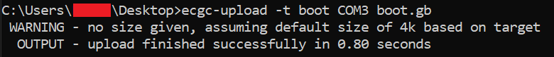
I ran ecgc-upload to test the new speeds, and holy moley.
The performance difference is night and day.
I've added a screenshot of the new scripts and it now takes around ~800 ms to re-program the boot ROM.
That's 4-5 times faster.
Pretty good, if I do say so myself.
With the new debug interface,
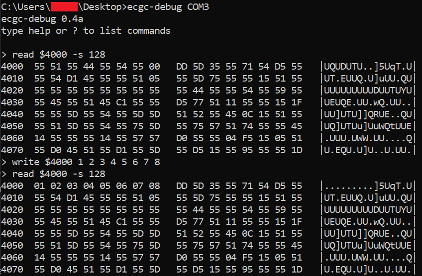
I also write a new tool ecgc-debug.
It allows me to read from and write to arbitrary memory locations in a CLI.
This allows me to test registers via the PC,
instead of having to write an assembly program to do it.
I've included a screenshot of an example below.
Here, I write a pattern to the PSRAM and check if the pattern was written correctly.
With these new debugging architecture and tools, I'll have an easier time testing and debugging, which makes this whole process much less painful. Dare I say it, I am almost looking forward to debug a weird random bug just to use these tools.
PSRAM controller
Speaking of PSRAM,
I installed the controller core I was developing in the previous post.
And it almost worked immediately.
I had somehow forgotten to drive the data lines when writing data to RAM.
After I found out however,
the issue was quickly fixed.
The core is now connected in the same manner it was connected to the MBCH previously
and still accessible at addresses $4000-$7FFF when using MBCH.
I also updated the DRAM tests I wrote for the Gameboy. Although, I can't call them DRAM tests anymore, can I? To reduce confusion, I changed the DRAM name to XRAM (which stands for eXternal RAM). This should also save me from changing the name again if I change the RAM technology in the future.
Anyhow, I ran the same tests again with the new controller and RAM.
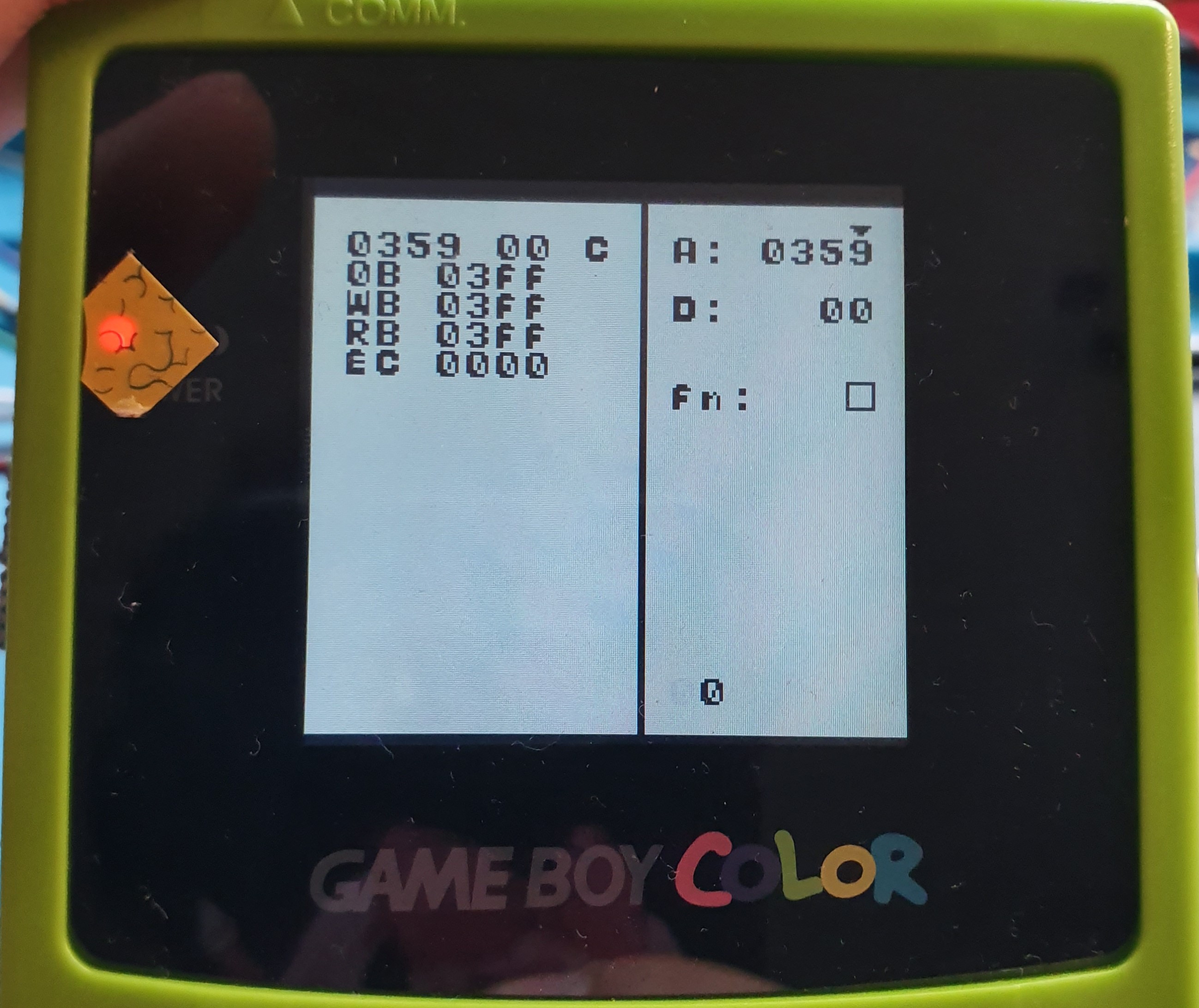
I have the results below.
Read this post to get information on how to read the test results.
TLDR; the number behind EC is the Error Count,
which should obviously be 0.
This time, I let the test run for all 1024 banks,
since it did not detect even one error!
Yippie!
With the new hardware iteration, the RAM chip is close to the FPGA and wired properly on a PCB, which should have eliminated any noise issues I had previously. The timing is also much more consistent now, due to the SRAM-like accessing method. The chip I use has an access latency of 70 ns. Coupled with the firmware delay, in simulations a read transaction from XRAM takes 140 ns currently. This is well under the 250 ns target for normal bus speeds and might be enough for double speed. I'll test that at a later date, but I have good hopes.
Bus redesign
One of the things I also worked on was redesigning the system bus. This relates to how all of the blocks are connected to each other in the cartridge. I was porting VHDL I had written for Gen3, but I ran into timing issues during PAR (Placement And Routing). It was mostly complaining about not reaching timing on the MBCH inputs. At first I was shocked since I've never had timing issues when working on Gen3, but then I remembered that Gen4 has a much higher clock (from 52.3MHz on Gen3 to 100MHz on Gen4).
Anyhow, to explain the issues I have provided a visual below. It is a diagram of the entire firmware with relevant external components.=

The timing issues arose from setup violations between the outputs of the decoder and the inputs of MBCH. This meant that the path between these two entities was too long, meaning that the changing outputs of decoder would not arrive in time at the MBCH inputs. I looked at the PAR reports and gave me a long, long list of components. The Wishbone bus had to travel through like 20 components, no wonder timing was not achieved. To remedy this, I experimented with cutting the logic path using registers. This would introduce some clock delay in the logic, but so be it.
For the uninitiated,
Wishbone has a handshaking protocol with its CYC and ACK signals.
When both these signals are high on a clock edge,
a handshake is made and the transfer of data is confirmed.
If one puts registers in between the communicating components,
it introduces 2 clock cycles of clock delay.
I've provided a visual to illustrate this below.
It shows a wave diagram of the supposed registered intermediary,
with i_cyc and o_ack connected to a master and o_cyc and i_ack to a slave.
Here, we also assume that the slave responses in 1 clock cycle.

As can be seen from the graphic at the left signals, the handshaking occurs much later then normal. This makes me a bit reluctant to include these stages in the design. If we were to register all crossbars for example, it would introduce 6 additional clock cycles of delay (60 ns with the current clock speed) for the Gameboy to get something from XRAM. Not to mention the bus decoding and the XRAM access delay. This could quickly spiral out of control and make the timings impossible for the Gameboy to get its data in time. Or we might be fine with Normal speed, but have trouble with Double speed.
Thus to decrease the delay, I changed the architecture a bit. Mainly, I put the crossbars inside the components that used them. This enabled me to cut out some delays. See the diagram below for the new bus design.

First, take the decoder crossbar, which now sits inside the Gameboy decoder. From it, it can communicate with the DMA core and all MBCs. The decoder uses a state machine to look at the Gameboy bus and decode the memory operations. In its state machine, I've now added the address and selected MBC decoding. This selects which bus connection is used to communicate with the appropriate slave. This topology eliminates the need to register the crossbar, since the assignments are already being done in a state machine, which is a clocked process.
The central crossbar now becomes the MBCH crossbar and is only connected to the MBCH.
Additionally, the crossbar registers the incoming Wishbone signals,
but outputs the acknowledgement directly.
This only increases the delay by 1 cycle.
For reference, look at Figure 5 and imagine that i_ack connects directly to o_ack.
Since the crossbar now connects only to MBCH,
the other MBCs are not accessible by the DMA and debug core.
However, there really wasn't any need to.
The DMA is a feature specific only to my cartridge and would therefore not be known of with other MBCs.
And debug core is only used to test stuff on the cartridge.
I don't need it to access other MBCs,
since everything is already accessible from MBCH (e.g. SPI, Boot ROM, Cart RAM, you name it).
Lastly, the XRAM crossbar. I haven't had any need to make it yet since I currently only have the MBCH, but I plan to to the same as with the MBCH. Depending on the slack I have with multiplexing busses, I will determine if I need to register the Wishbone bus. Although I am guessing I'll need to at least register the incoming signals and can just provide ACK directly. But that's something to think about when I get there.
Overall, the system has become more monolithic. However, the reduced latency is worth this.
Closing remarks
So yeah, firmware progress is going slow and steady. I also have no reason to deviate from the plans set in the last post, so next step will be to implement SPI. Although, I think after that I will focus on the SPI software rather then more firmware. I haven't had much chance to spend on software, since I mostly had to spend it on hardware and firmware (can't write software without a platform).
For the software I still have a bunch to implement, including but not limited to:
- SPI driver
- NOR flash driver
- RTC driver
- SD card disk I/O
- Filesystem stuff
Also, a quick update of my personal life. I have finally graduated in my bachelor and will be entering the workforce on the first of March. That means that I will be busy again, so keep that in mind when I eventually post next year /s. I do hope to spend an hour here and there on the project, but I can't promise any timelines: I'll get to it if I have the time and energy. After all, what's the use of a project you're doing for fun if you don't have fun :)