
Project:
ecgc
Date:
16/09/2022
Working DRAM + test/debugging application + SPI controller access
Starting with college again after a busy summer vacation. I was able to add a few stuff to the project:
- Working link with DRAM used for program memory
- Wrote memory debugging app for boot ROM
- Added access to SPI peripheral via WishBone bus
I am also in luck, since I am able to work on the project for school. We have to do a personal project 1 day a week, so obviously I grabbed my chance to continue working on this project. I'll explain later in more detail what I'll do with my time.
Working DRAM
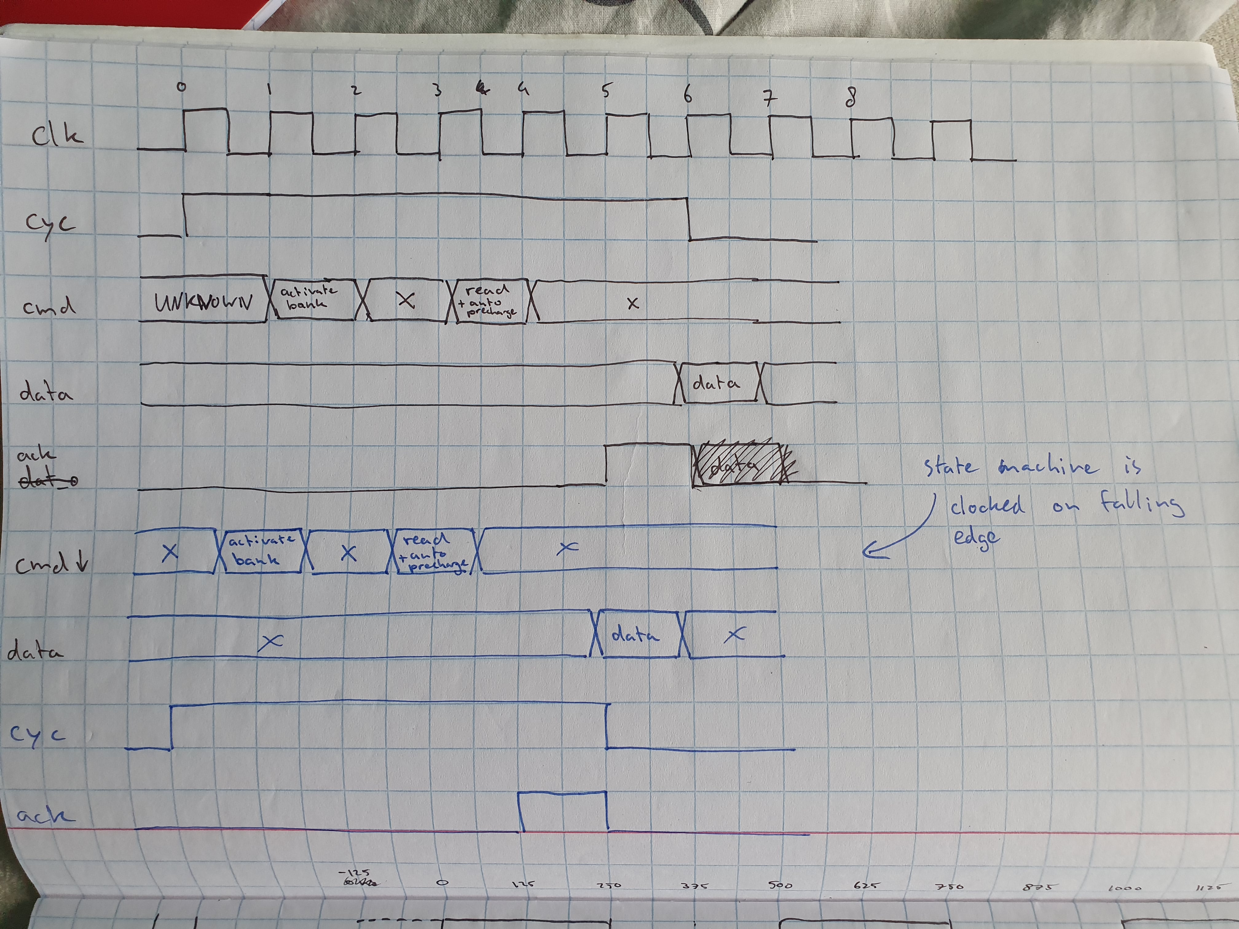
I've added the last must-have chip to the prototype: the DRAM. This DRAM chip will contain the currently running program loaded in from the SD card. I wrote a DRAM controller which converts WishBone transactions to DRAM commands in sequence.
The current implementation works, but has a very high latency. Currently this is not an issue and performing R/W operations falls within acceptable bounds. However, I have little hope that current implementation can handle the Gameboy Color double speed mode.
I wrote some notes to keep track of the procedure done during memory operations:
To read:
1. Send Activate Bank
2. Wait for Trcd (21 ns = 2 clocks)
3. Send Read with Auto Precharge
4. Wait for CAS delay (2 clocks)
5. Read data from DQ lines

To write:
1. Send Activate Bank
2. Wait for Trcd (21 ns = 2 clocks)
3. Send Write with Auto Precharge (including data on DQ lines)

To auto charge (must be done once every ~7.8 ms):
1. Send Auto Refresh command
2. Send NOP till finished (min. Trc = 4 clocks)
3. Send NOP till finished (min. Trc = 4 clocks)
4. Send NOP till finished (min. Trc = 4 clocks)
5. (Free for something else)

Possible timing issues:
    -   Having to do a refresh while a cart access is being made
        can royally screw us.
    -   Bank activate could take some time

Possible replacement:
https://nl.mouser.com/ProductDetail/Alliance-Memory/AS1C8M16PL-70BIN?qs=byeeYqUIh0NST7XYuCr8lQ%3D%3D
As can be seen, Read operations takes 5 clock cycles to complete. With the current speed (53.2 MHz), this would result in a memory latency of ~94 ns. Looking at the timing diagram below, it can be found that worst case I have 68 ns and best case 193 ns. This difference has to do with whether the Gameboy reads the data on the bus at the falling edge or in the middle of the falling to rising edge of GB_CLK. From preliminary testing, it seems to be the latter (ie. writing and reading to DRAM a couple of times). But is to be investigated further.
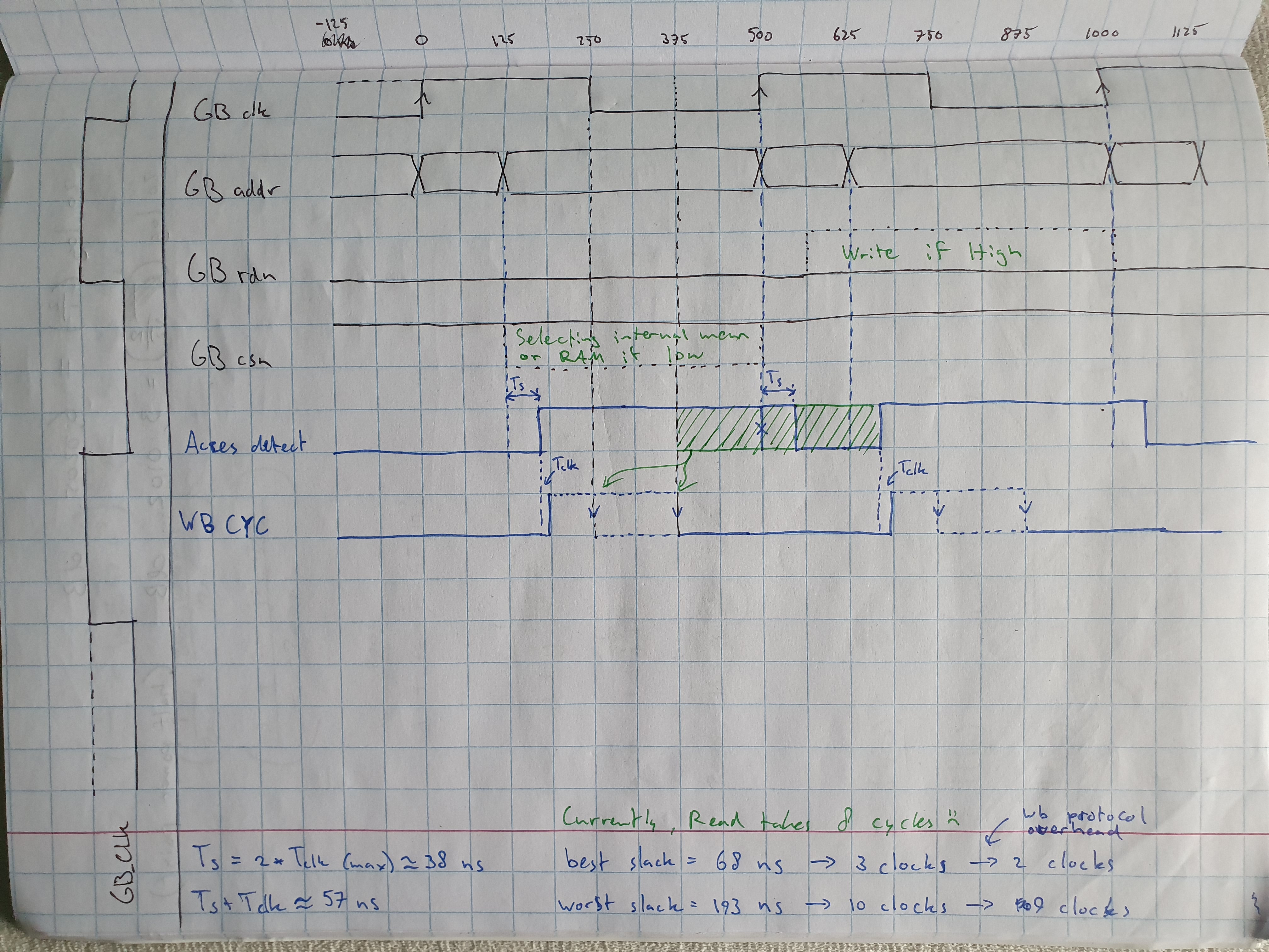
I was able to shorten the latency of the DRAM state machine by 1 clock cycle by clocking the state machine with the falling edge (see image below). I don't know if I can shorten the latency any further, so I should test the current implementation against double speed mode.
In the case of failure, I might have to go with SRAM after all. It has more predictable timings, which seems to be necessary in this system where the CPU cannot stall because of memory latency. I found a component that is relatively cheap, but it is a BGA package. But I'll look further into possbile replacements when the time comes.
Test application
I also spent time into developing an application to test memory. It is a simple application which allows me to pick a memory location. I can then read from or write to that location. The application also shows a history of the last few transactions, to make it a bit easier to work with. A screenshot is included below.
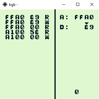
The controls are quite simple:
| Buttons | Action |
|---|---|
| Left + Right | Select address and data nibble (the cursor wraps around). |
| Up + Down | Change value of hexadecimal nibble (the value wraps around). |
| A | Read from memory location behind "A :" |
| B | Write value behind "D :" to memory location behind "A :" |
The application also moves the character "0" across the bottom of the screen to show that the Gameboy is still running.
The application runs from boot memory. It was easiest to put it on there, but it currently disrupts the actual function of the boot ROM by being quite large.
SPI peripheral
I was also able to hook up the EFB block of the FPGA to the WishBone bus.
This allows the Gameboy to access the EFB block at address 0xA000-0xA0FF.
See the Using Hardened Control Functions in MachXO3D Devices Reference Guide for specific addresses on the EFB peripherals.
I've currently only used it to access the SPI peripheral for use with the SD card.
It works well, except for the speed.
The SPI clock comes from the internal oscillator, which is then pre-scaled by a pre-scaler register (0xA057).
However, even at the largest pre-scaler of 0x3F the clock is still too fast according to the SD card specification.
The specification mentions a max. SPI frequency of 400 kHz at initialisation. This speed can then be increased after querying the card type, but it has to be < 400 kHz at startup. Doing the math, our 53.2 MHz clock is divided by 64 creating a ~800 kHz clock, As this is out of spec, this has to be fixed.
School project
As I said initially, I will be working on this project during my time at school (hurray!). Specifically, I'll be working on an issue I'm seeing as I'm developing the boot ROM.
Uploading code to the boot ROM is very tedious, so development/testing is very time consuming. The boot ROM is programmed alongside the FPGA fabric, so changing a line in the code means recompiling and uploading the entire FPGA. This takes multiple clicks and ~2 min of waiting, which adds up after 50 code changes.
To solve this problem, I wanted to develop a system which allows me to directly modify the boot ROM (or program RAM) while the firmware continues running. This would allow me to quickly push code changes and make development easier.
Ideally, I'd want to be able to access the memories via JTAG, but I could also add a serial port or something.
Some closing remarks
During my time at school, I have to keep regularly updating my teacher. I plan to just use this website, so expect a post every 3 weeks.
I'll be focussing on the code uploading issue during this time.