
Project:
ecgc
Date:
01/06/2022
First working prototype
My first post on this project and on this website, so exciting! I wanted to report on the current progress of the project. As mentioned on the project page, I started making this website after having made my first working prototype. I've been busy for a month making this website, so I haven't been busy with the project.
Also, it's nearing the end of my internship, so I can't continue immediately after this post. I plan to continue in the summer vacation. I basically have the entire month of July to work non-stop, so that's probably what I'll do. For now, I wanted to use this post to detail the current progress + explain how the prototype functions before I forget.
The design (thus far)
I thought to first explain what my planned design is, before moving on to the current prototype.
The plan is to make a cart based around an FPGA/CLPD (continuing in this document, I'm just going to refer to a CLPD). This CLPD will decode whatever the Gameboy puts on its bus and perform the requested reads/writes. I've provided a block diagram of this system below.

The area outlined is the CLPD architecture implementation. It will contain a Gameboy decoder block to convert the Gameboy specific bus commands to WishBone. Wishbone is an open standard for CLPD interconnects The chip I'm using has some hard core peripherals exposed to an Wishbone bus. Using WishBone, I can design an architecture to enable the Gameboy to access these peripherals.
The most important of these interfaces is the SPI controller. It will be used to communicate with the SD card using the SPI protocol. I also plan to include some accelerator functions in the controller (eg. CRC calculation/verification, command building), but we'll see what fits.
The SD card will contain the games to play on the Gameboy. It will also contain other non-volatile data, such as menu themes, splash-screen, game saves, anything your heart desires. I plan to make the card bootable, with the boot partition containing a pointer to a bootloader. This bootloader should contain code to interpret the filesystem on the SD card and load the menu program, along with theme information. Using a bootloader setup should allow users to patch bugs, without needing to reprogram the CLPD.
To load the bootloader however, the Gameboy must know how to use the SPI peripheral to read from the SD card (and load the bootloader). The cart must have a minimal program ran at boot to accomplish this. The CLPD I use contains a few kB of flash storage I can use for this purpose. When the Gameboy first boots, it should immediately read from this flash to kick-start the boot procedure. This code should be written carefully, since updating it requires re-flashing the CLPD which one can only do with a JTAG programmer. It goes without saying, but I don't expect the general consumer to have one.
The last crucial part is the DRAM. Its job is to store the program currently ran by the Gameboy for it to be able to access. The Gameboy has some strict bus timings it needs to adhere to and the program memory needs to be accessible on time. RAM is perfect for this job.
I'm still not sure about the inclusion of a DMA peripheral. It should be really handy for fast copying of data from the SD card to DRAM (or when saving game saves, copying data from DRAM to the SD card). The Gameboy performing this copy action would be insane slow (I think), since the Gameboy runs at a fraction of the Wishbone bus speed.. I think it is also necessary for copying the kick-start program from user flash to DRAM. I am not sure if the user flash interface is fast enough to guarantee the bus timings of the Gameboy. If it is not able to adhere to these timings, I need a peripheral that is able to throttle itself while copying this data.
Current prototype
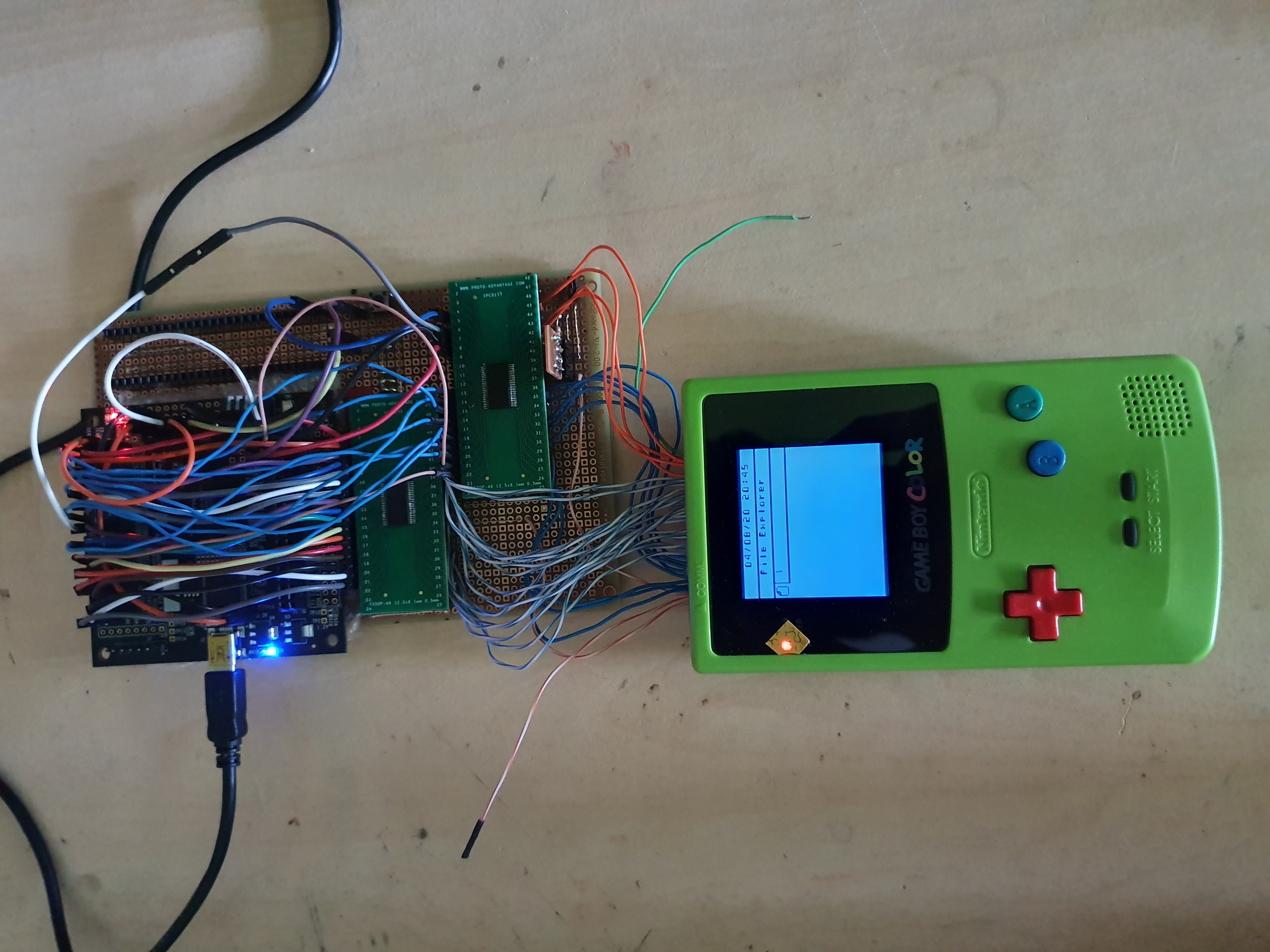
The current prototype is functional (somewhat). Here it is running my very first program. This program is a start to the file navigator for manipulating the filesystem on the SD card. The looks aren't final though. It was my first ever program, so I experimented a lot with drawing to the screen.
The functional side
This was the first firmware-based prototype, it it mainly exists to prove the viability of this approach. I am a beginner when it comes to firmware and FPGAs, so it was also a test of my own skill. Luckily, it works. I've provided a functional block diagram of the current system below.

The decoder will convert Gameboy-speak to WishBone. WishBone is then used to read from internal ROM. The prototype uses internal BRAM as ROM for storing the program. The memory is programmed with a given image automatically at startup, before the CLPD initialises.
This memory is easy to use in firmware and therefore ideal for testing. To test it, I simply flashed a small Gameboy program to it and boot the sucker. This is what you see in Figure 2.
There are some obvious problems with this approach though for release. This was of course never intended as a release, but here are the problems anyways:
- The internal ROM is very small (4kB). I could make it a bit bigger, but even using all internal ROM, it would still not be able to fit the smallest Gameboy games (which are 32kB). Additionally, the largest game theoretically possible using the most capable MBC is 8MB (taken from Wikipedia).
- The game has to be flashed along with the CLPD. This means that one has to resynthesize, reimplement and reflash the entire CLPD code + converting the desired game to the .mem format when changing games. This is of course, incredibly impractical.
The prototype is still a success though, since I was able to test the decoder. I took the Game Boy: Complete Technical Reference - Appendix C as a reference. I wasn't sure if my implementation would work, so I wanted to quickly test it.
Used CLPD
The prototype is based around the Lattice MachXO3D family of CLPDs. The MachXO3D seems a bit overkill for my application (and it is). However, it was the cheapest, usable CLPD I could find at the time. There is also a chip shortage currently, so I'm out of other options.
Originally, I went for the Lattice MachX02, which has less features and is cheaper, but I can't buy it anywhere. I chose the MachXO3D, since it was available at the time and it's kinda compatible with the MachXO2.
Here's a short list of other reasons:
- Both have built-in SPI. This is necessary for communicating with the SD card.
- Both have internal flash storage. This is handy for saving the kickstarter and/or configuration data. It saves having to include external flash memory.
- Both have enough IO pins. I need enough for communicating with the Gameboy (~30 pins), DRAM (~30 pins), SD card (4 pins) and other possible peripherals. In total, I need about 70 pins.
There are some problems however with the MachXO3D:
- The MachXO2 has DDR support, the MachXO3D not. This would save me the hassle of implementing a DRAM controller in the CLPD fabric. It does seem interesting to write one though, so I'll bite.
- The MachXO3D has some unnecessary features (primarily a ton of security features). This is completely useless for the cartridge. No sane hacker will try to convince you to play a spoofed game, since the Gameboy has no connectivity and contains no user data. The worst they could do is destroy the save data on the SD card, but why would anyone bother.
Despite these issues, I went ahead with the MachXO3D. I does enable me to write and test large parts of the firmware (SD card controller, flash interface, Gameboy bus decoder, etc.).
The electrical side
The abomination of wires below is the culmination of my suffering.
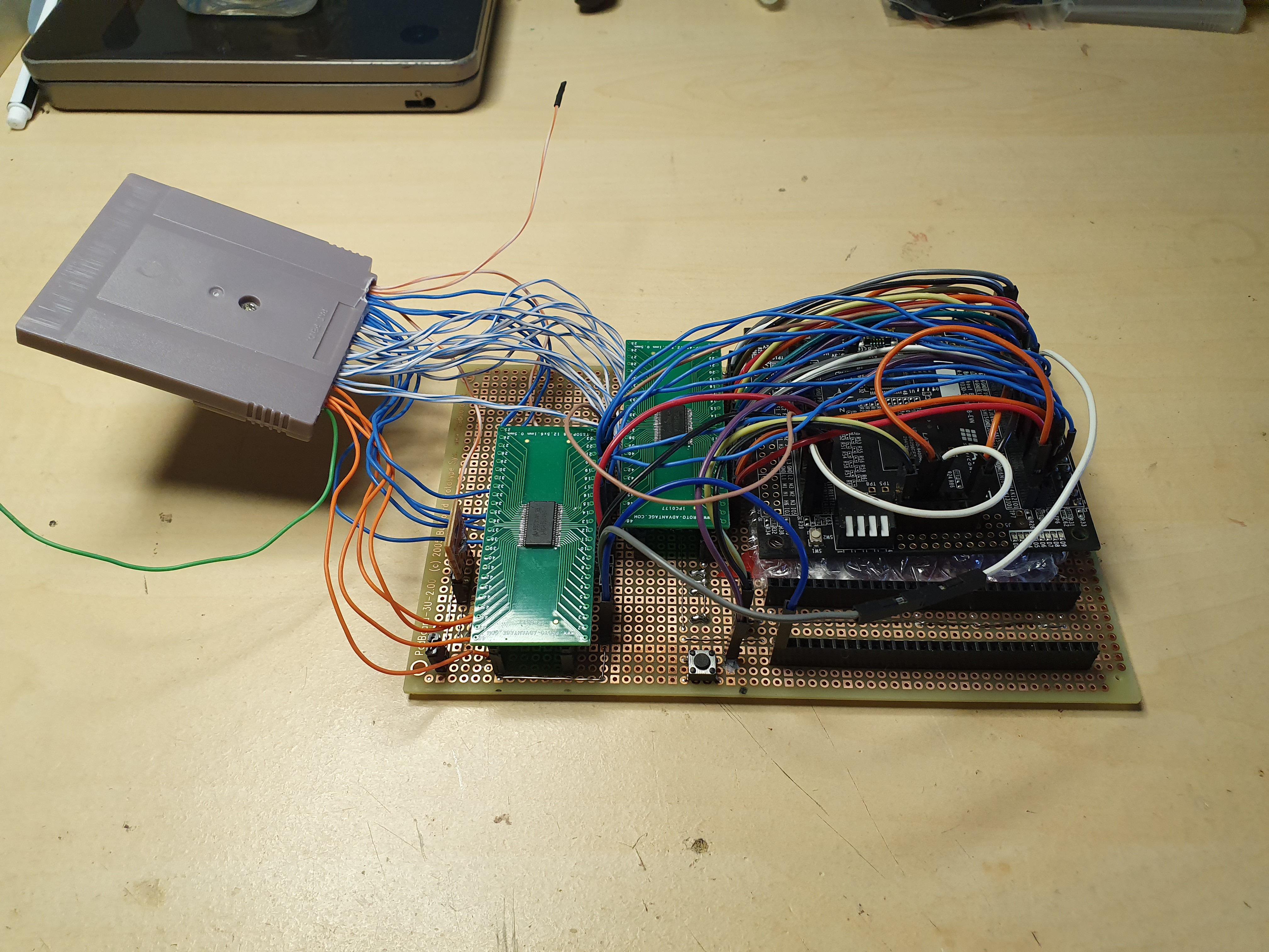
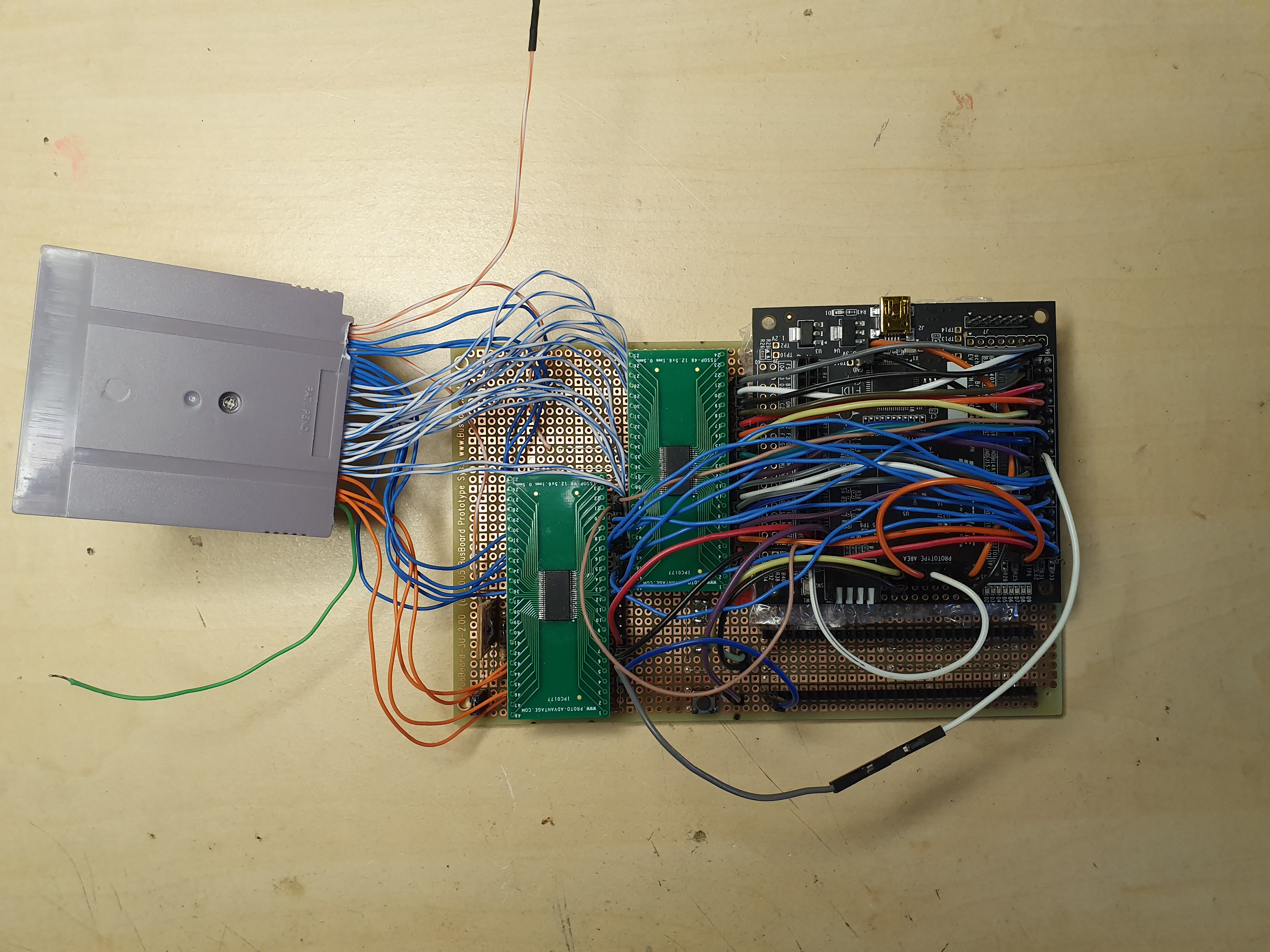
The large black PCB is the MachXO3D breakout board. It has a LCMXO3D-9400HC-5BG256C CLPD in the middle, with some supporting hardware (voltage regulator, JTAG-to-USB converter chip, etc.). Most importantly, it has big round holes I can solder wires to (if you look closely, you can even see these wires). The solder holes to the side of the board are IO from the CLPD. These can be routed inside the CLPD to perform any number of logical functions.
The 2 green PCBs with a single chip are bus transceivers. The Gameboy works with 5V TTL logic levels, while the CLPD works with 3.3V CMOS levels. I found out that TTL is an older standard and modern components are rare to abide by it. It was impossible to find necessary components working with 5V levels. Instead, I opted to go the conversion route. The bus transceivers functions as level shifters, down-translating the 5V TLL to 3.3V CMOS. The transceivers do not up-translate the voltage, but 3.3V is seen as a logical '1' by TTL standards so this is not an issue.
I did have some reset issues using 3.3V. My after market screen would stay in reset when issuing a reset from the cartridge. To solve this, I added a dedicated level shifter to the reset pin. This will buffer the 3.3V signal to 5V. After testing it with my screen, I no longer have flickering issues.
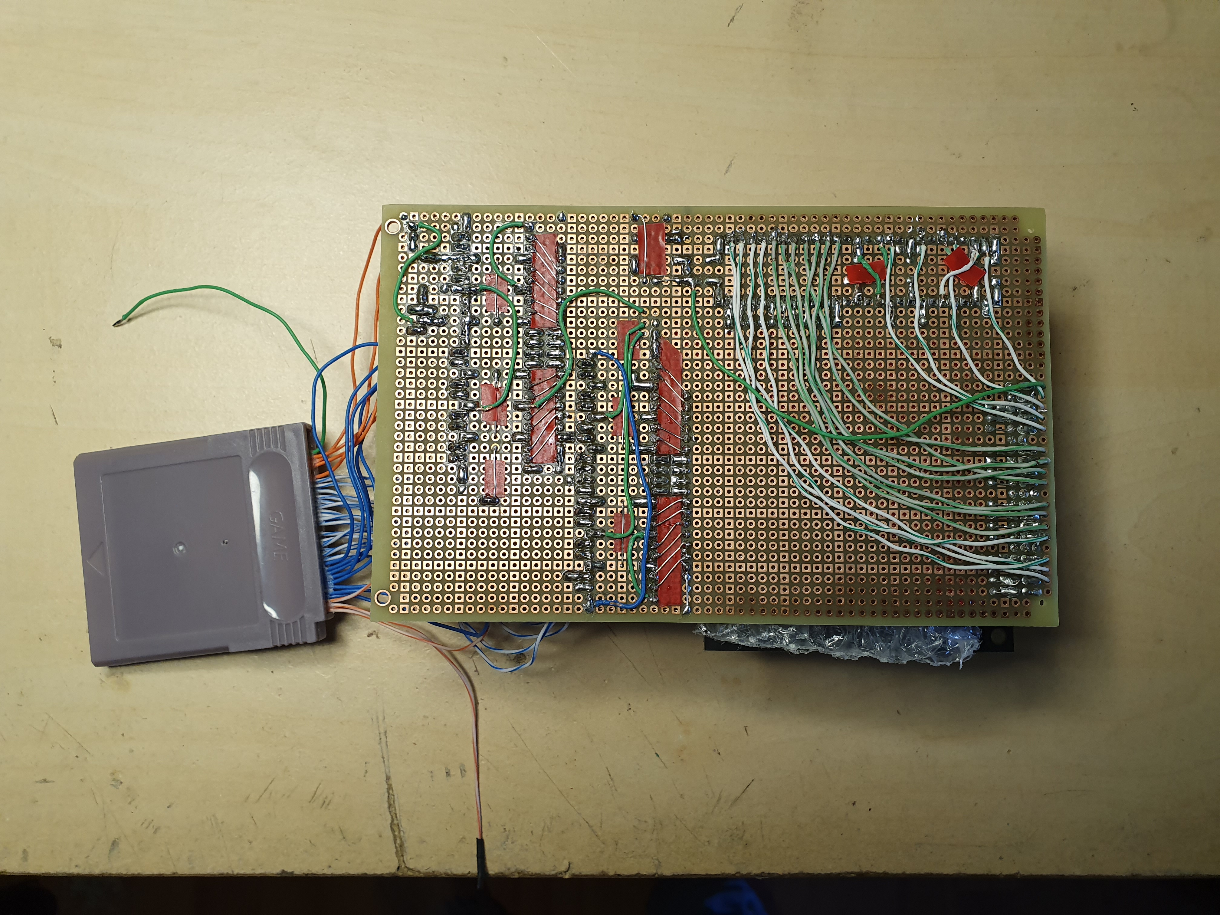
Back to the bus transceivers. The other side is connected to the cartridge pins. I used a PCB of a previous prototype and soldered some cables to it. It's not pretty, but it does the job.
The empty socket is reserved for the DRAM chip. It is currently being used as a convenient ground.
Previous prototypes
The project is quite old (it's been almost 2 years now) and I've designed 2 prototypes till now. Since I come from a background in software engineering, I spent this time attempting to drive the cart via some software magic. Honestly, the first attempts were absolute crap and were doomed to fail. I did learn about the process, so it's safe to say it wasn't completely useless.
1. Breakout board for an MCU
With the first one, I tried designing the PCB first. I planned to make a breakout PCB only containing the bus transceivers, memory chips, reset level shifter and a voltage regulator. See below for the PCB.
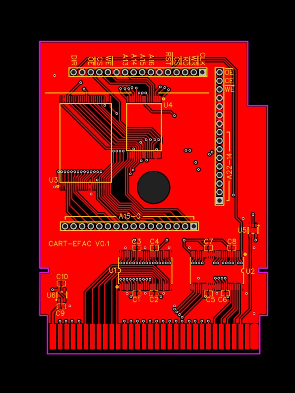
I must've snorted the wrong stuff however, because I completely forgot to route holes for the Gameboy data signals. These are 8 separate wires, so I have no idea how I've missed them. Because of this, the PCB was completely useless and I utterly embarrassed myself.
The PCB was also manufactured too thick. I kept it at the standard size when ordering, which was a mistake. Because of this, the cart would not slide in the cart slot.
2. Modular prototype
In the second prototype, I though about making it modular. The reason being that, at the time, I was planning to use SRAM as game storage. The chip I used however was ridiculously expensive (~€26 per chip). Since I didn't want to "waste" a €26 chip every time I changed designs, I wanted to make a modular daughterboard for it.
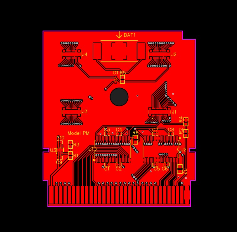
The motherboard would have the cartridge contacts, power electronics, bus transceivers and the reset hardware. Then, I would make 2 daughterboards which I could swap: one for memory and one for the MCU. This would also allow me to make different revisions of the board (eg. daughterboard with less memory).
It did have some issues though. When I designed the motherboard, I added 2 connectors per daughterboard. I did this for 2 reasons:
- distribute the signals signals by allowing them to come from 2 sides
- better mechanical stability
This quickly became an issue while soldering. I had to solder the connectors in exactly the right position for the daughterboard to fit. If one of the connectors was even slightly off place, I couldn't connect the board. I broke the connectors while soldering and I eventually gave up.
I did route the data lines this time though, so I at least have that...
Change in approach
While failing, I did learn to change my approach in developing the hardware.
For the current prototype, I've opted to ditch trying to make everything fit inside the cartridge. Now I have everything messily connected on a perforated board. This allows me to make changes on the fly as I prototype. At the time of writing, I've already identified and fixed several issues (wrong port routings, the reset level shifter).
After implementing and testing the firmware on this prototype, I can really focus on miniaturising everything knowing it works (provided I don't mess up the PCB design).
Some closing remarks
This post is kind of an information dump. It's the first post on my site and I basically summarise a process which started 2 years ago. In the future, I plan to make more frequent, smaller posts. But for now, please bare with me.
And if anyone is reading this, I hope my future endeavors interest you and you keep reading these. Thanks for reading!